Polarizers

Wire-Grid Polarizers

Moxtek® polarizers & beam splitters are the preferred choice for many applications that demand performance, wide angle of incidence, and temperature durability. Moxtek® broadband products are built using state-of-the-art nano-scale patterning technology.
AOI
Large angle accapance
λ
Broadband

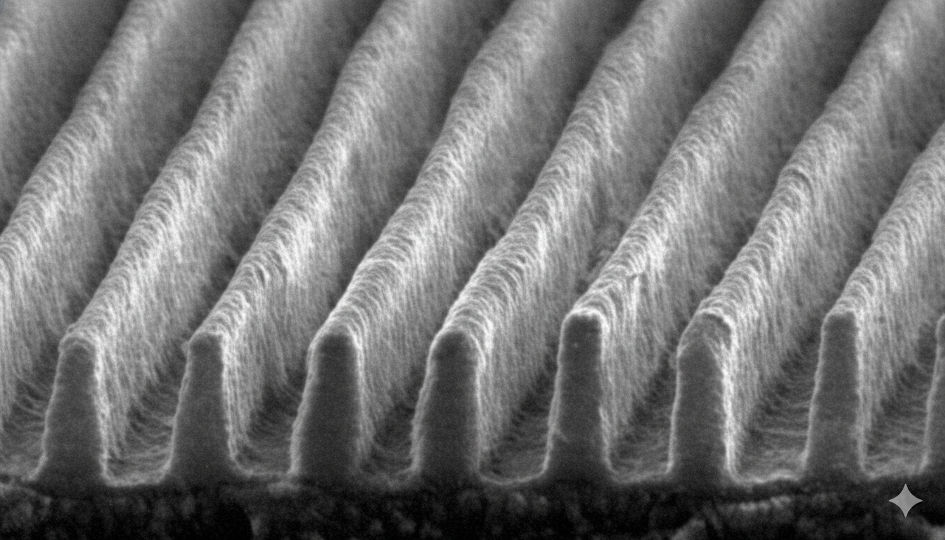
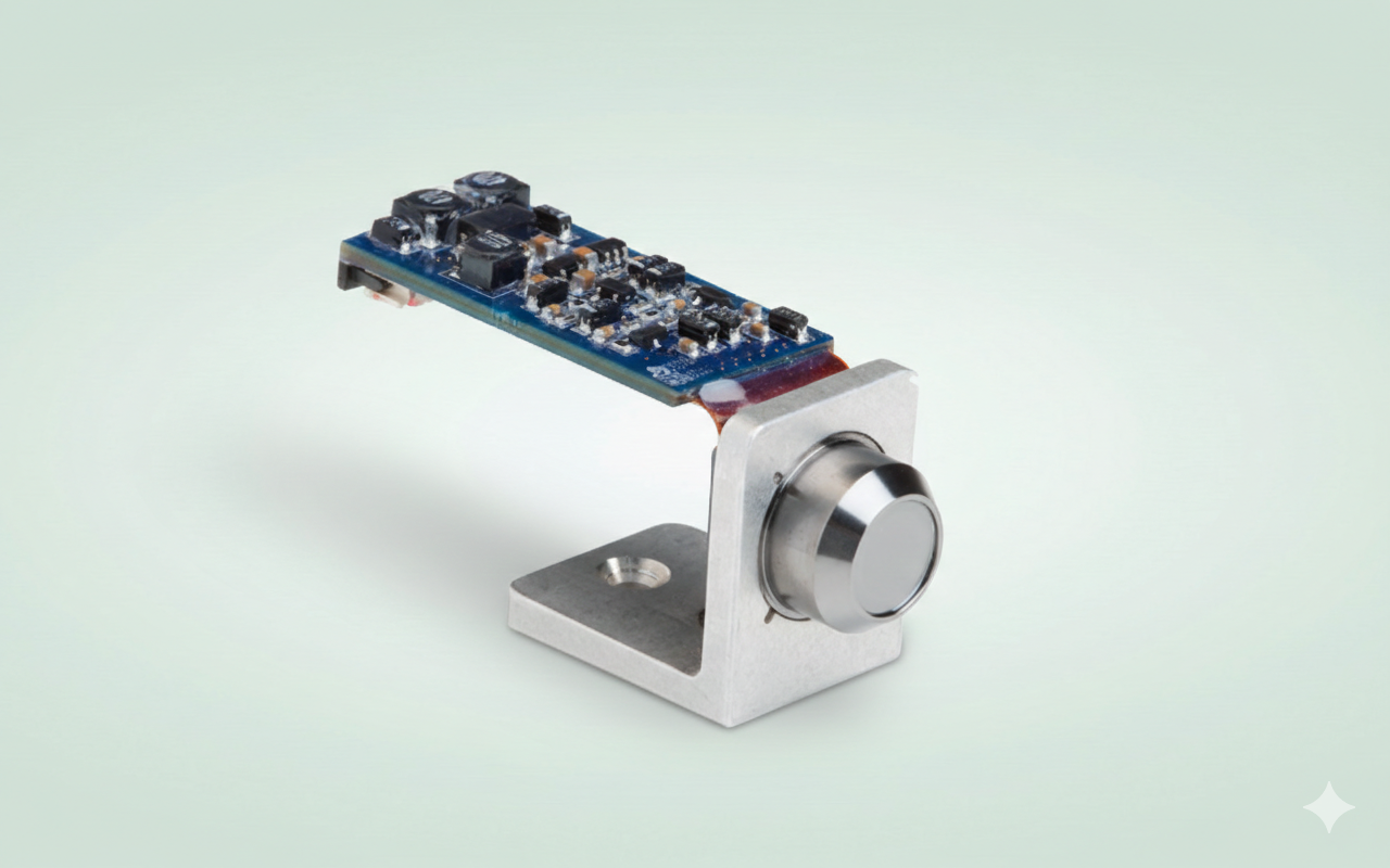
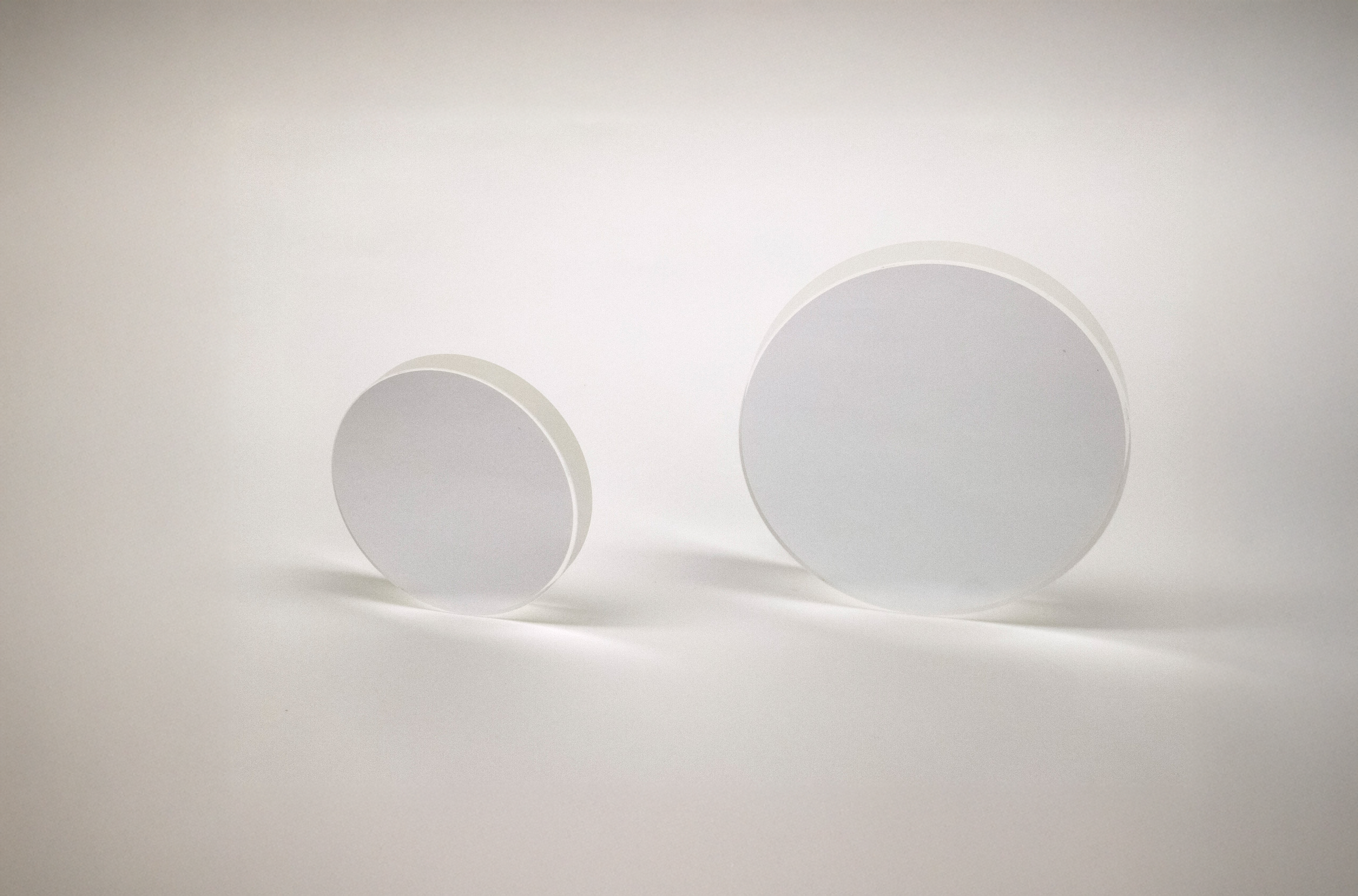
Moxtek wire-grid polarizers are advanced nanostructured optical components designed to provide exceptional polarization control across a very wide spectral range, from the ultraviolet through the infrared. Using subwavelength aluminum nanowire technology deposited on robust substrates, these polarizers efficiently transmit one polarization state while reflecting the orthogonal state, achieving high extinction ratios and excellent transmission over a broad range of wavelengths and angles of incidence (AOI).

Engineered for both performance and durability, Moxtek’s polarizers maintain stable optical characteristics under high temperatures, humidity, and UV exposure, making them ideal for projection systems, imaging, spectroscopy, machine vision, and scientific instruments. Their compact, thin-film construction allows seamless integration into complex optical assemblies where wide field-of-view and environmental resilience are critical.

In short, Moxtek wire-grid polarizers combine broadband operation, wide AOI tolerance, and rugged reliability, setting the standard for modern polarization optics.

not sure what fits?

Let us help you

We love to solve this puzzle and find the right fit.
Heading for types of this product
Green Architecture
Evermind™ template is crafted like sustainable structures — clean, scalable, and built to last.
Precision Engineering
Every layout and component is tuned with variables and pixel-perfect details, so your brand stands on solid ground.
Dynamic Interactions
From nature-inspired transitions to fluid page structures, Evermind™ feels alive yet quietly sophisticated.

Foundry Services

Moxtek collaborates with customers to design, verify, and create solutions for high-volume manufacturing. They provide options for prompt design iterations and NanoImprint Lithography (NIL) optimization. Moxtek uses Statistical Process Control (SPC) monitoring of post-print Critical Dimension (CD) repeatability.

Moxtek offers prototyping samples through their recurring Design Master Shuttle. This NIL Design Master Shuttle includes space for multiple (different) design structures, allowing engineers to test several designs on a single shuttle iteration, thereby reducing development time and cost. They can add a customer’s unique design to their next Design Master Shuttle for prototyping the latest lens or nanostructure optical device. These design shuttles are processed multiple times each year.

Moxtek has been producing nanostructured optical components for over 20 years. They offer high-volume wafer replication of nanostructure devices on Ø200 mm wafers. Their versatile capabilities are used to manufacture functional metasurfaces, including metalenses, meta-optical elements (MOE), diffractive optical elements (DOE), patterned nanostructures, waveguides, photonic crystals, and biosensor arrays. These devices are used in imaging, illumination, and display systems for a wide range of applications, including automotive, medical and dental imaging, camera systems, and many others.

Download Datasheet

Benefits

Moxtek wire grid polarizers provide exceptional optical performance across a wide range of conditions.

  • Uniform Transmission & Reflection
  • High Transmission, High Contrast
  • Wavelength Independent
  • Wide Angle of Incidence
  • High Temperature Durability

Benefits

Moxtek wire grid polarizers provide exceptional optical performance across a wide range of conditions.

  • Uniform Transmission & Reflection
  • High Transmission, High Contrast
  • Wavelength Independent
  • Wide Angle of Incidence
  • High Temperature Durability

Benefits

Moxtek wire grid polarizers provide exceptional optical performance across a wide range of conditions.

  • Uniform Transmission & Reflection
  • High Transmission, High Contrast
  • Wavelength Independent
  • Wide Angle of Incidence
  • High Temperature Durability

Contact Us for Free Consultation
Related products
Related News For this Product
No items found.
ready to start?
Stuck with a spec sheet that reads like sci-fi? Need a component that probably doesn't exist yet? Let's make it happen. Together.
FAQ

Questions, answered with clarity.

We’ve collected the questions we get all the time, and actually answered them. No mystery, no marketing poetry - just facts. Still have an open question? We're here to help:
Contact Us
Advanced Nanostructured Optics and Polarization Solutions
What materials are used in the wire-grid polarizers?

The grids are made of inorganic aluminium nanowires patterned on glass, fused silica or silicon substrates.

What wavelength ranges do they cover?

They have broad coverage. For example the Ultra Broadband version covers ~300 nm up to >4 µm. For IR versions: 3-12 µm are available. For UV it's down to 240nm.

What’s the maximum temperature / durability?

They are heat-tolerant (for example rated >200 °C for >5,000 hours in certain series).

What is the angle of incidence (AOI) tolerance?

They accept wide angles – many types accept ±20° without performance loss.

What handling or cleaning precautions are needed?

The grid structure is delicate - Do not touch or clean the wire-grid polarizer surface otherwise the polarizer will be damaged!

What’s the advantage over a polymer-film polarizer?

The inorganic wire-grid design offers higher durability, better temperature/brightness tolerance, and broad bandwidth performance.

New Products
Facing a Challenge? Let’s Solve It Together