Foundry Services
Moxtek collaborates with customers to design, verify, and create solutions for high-volume manufacturing. They provide options for prompt design iterations and NanoImprint Lithography (NIL) optimization. Moxtek uses Statistical Process Control (SPC) monitoring of post-print Critical Dimension (CD) repeatability.
Moxtek offers prototyping samples through their recurring Design Master Shuttle. This NIL Design Master Shuttle includes space for multiple (different) design structures, allowing engineers to test several designs on a single shuttle iteration, thereby reducing development time and cost. They can add a customer’s unique design to their next Design Master Shuttle for prototyping the latest lens or nanostructure optical device. These design shuttles are processed multiple times each year.
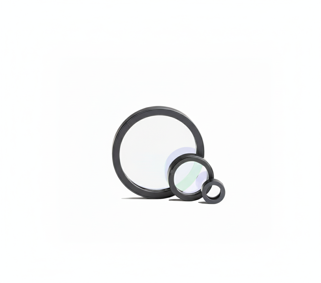
Moxtek has been producing nanostructured optical components for over 20 years. They offer high-volume wafer replication of nanostructure devices on Ø200 mm wafers. Their versatile capabilities are used to manufacture functional metasurfaces, including metalenses, meta-optical elements (MOE), diffractive optical elements (DOE), patterned nanostructures, waveguides, photonic crystals, and biosensor arrays. These devices are used in imaging, illumination, and display systems for a wide range of applications, including automotive, medical and dental imaging, camera systems, and many others.


.jpg)

.png)