polarizers

Metalens Foundry Service

Moxtek manufactures high-performance metalenses for visible and IR wavelengths. Moxtek offers a full solution, including design, fabrication, measurement, and packaging capabilities.
IR
visible

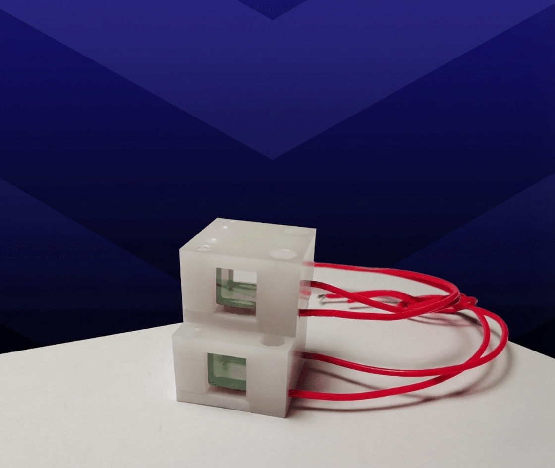
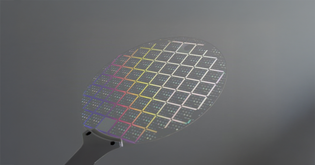
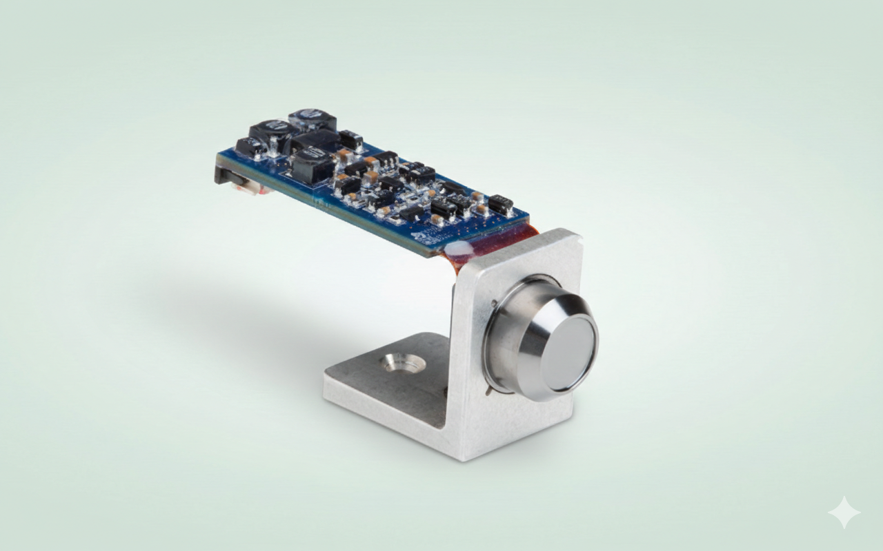
Metalens benefits include reduced track length and weight in optical systems. They can have more design flexibility, additional functionalities, shorter focal lengths and smaller diameters compared to traditional optics. Metalens micro-lens arrays (MLA’s) are also possible, with more design flexibility than traditional MLA approaches. As a meta- and nanostructured-optics company we have overcome various challenges associated with scaling up visible wavelength metalens manufacturing to production volumes. We have developed efficient methods to create replication masters combined with our existing NIL processing to provide a full solution approach to volume production. Moxtek replicates metalenses with extremely tight tolerances and high repeatability. Moxtek utilizes high aspect ratio etching into transparent films of high refractive index to achieve high performance metalenses.

not sure what fits?

Let us help you

We love to solve this puzzle and find the right fit.
Heading for types of this product
Green Architecture
Evermind™ template is crafted like sustainable structures — clean, scalable, and built to last.
Precision Engineering
Every layout and component is tuned with variables and pixel-perfect details, so your brand stands on solid ground.
Dynamic Interactions
From nature-inspired transitions to fluid page structures, Evermind™ feels alive yet quietly sophisticated.

Foundry Services

Moxtek collaborates with customers to design, verify, and create solutions for high-volume manufacturing. They provide options for prompt design iterations and NanoImprint Lithography (NIL) optimization. Moxtek uses Statistical Process Control (SPC) monitoring of post-print Critical Dimension (CD) repeatability.

Moxtek offers prototyping samples through their recurring Design Master Shuttle. This NIL Design Master Shuttle includes space for multiple (different) design structures, allowing engineers to test several designs on a single shuttle iteration, thereby reducing development time and cost. They can add a customer’s unique design to their next Design Master Shuttle for prototyping the latest lens or nanostructure optical device. These design shuttles are processed multiple times each year.

Moxtek has been producing nanostructured optical components for over 20 years. They offer high-volume wafer replication of nanostructure devices on Ø200 mm wafers. Their versatile capabilities are used to manufacture functional metasurfaces, including metalenses, meta-optical elements (MOE), diffractive optical elements (DOE), patterned nanostructures, waveguides, photonic crystals, and biosensor arrays. These devices are used in imaging, illumination, and display systems for a wide range of applications, including automotive, medical and dental imaging, camera systems, and many others.

Download Datasheet
Related products
No items found.
Related News For this Product
No items found.
ready to start?
Stuck with a spec sheet that reads like sci-fi? Need a component that probably doesn't exist yet? Let's make it happen. Together.
FAQ

Questions, answered with clarity.

We’ve collected the questions we get all the time, and actually answered them. No mystery, no marketing poetry - just facts. Still have an open question? We're here to help:
Contact Us
Advanced Nanostructured Optics and Polarization Solutions

New Products
Facing a Challenge? Let’s Solve It Together